

SSV
-
Posts
68 -
Joined
-
Last visited
Never
Content Type
Profiles
Forums
Downloads
Everything posted by SSV
-
I want to number one correlate device monitor with dna200 on-screen readings, vs external shunt (be it physical 1mV/A shunt, or the shunt in the dm3068). I typically use an external shunt to try and avoid DMM burdens etc, but I see your point about port output resistance....chances are under a fault condition the limiting factor is the physical nature of the port? I have had some issues with other on-board USB charging devices blowing out MOBO usb ports (fault conditions)....and I want to verify that under a fault condition this wouldn't happen with the dna200 (via USB charging). If we decide to package the chip with our wire profiles built in, I would like to offer customers a warranty and guarantee that charging is reliable. This seems to be the number one complaint about the dna200 right now (which I don't agree with at all) is that it's limited to the internal 3s pack and on board charging. I want to give any potential customers confidence, that the device is "safe" via USB. One good way to do that is simulate a fault condition and see if I can get the DNA200 to pull more than 500mA from an industry spec USB port (I typically see around 420mA when I do this test, but saw 480mA draw from the dna200 @ 4.4v). This 4.4v vs 480mA I saw in device monitor was the trigger that set this question off for me....at 4.4v 480mA is still within tolerance? If 4.4V bins the V as "low" shouldn't the current draw be reduced? Or is the controller fast enough to "bin" that low reading and say 480mA does not = 500mA, and is therefore an acceptable reduction of current for that scenario? You'll have to please excuse any lack of knowledge I have on USB specifics, as it's not my field or forte' (I don't deal much with serial related devices....I am mostly in DC/DC hardware...and a piss poor software engineer....I know enough about serial protocols and coding to be annoying, but far from implementation level knowledge). P.S. even in DCv setting on the DMM there is slight burden from the meter....I am not sure it's relevant to the granularity of measurement here, but I typically try and null all uncertainty from a DUT.....overkill? probably, but my background is in precision devices....so we have plenty of hardware here with overly fancy binding posts (IETlabs seems to have a large chunk of my bank account in their bank account). I'll strip down a few cables and give your test loop suggestions a try. P.P.S If USB spec device (linear reg side) sees a 4.4V signal....it should limit current to move back into it's safe "bin" correct?[/QUOTE]
-
I want to number one correlate device monitor with dna200 on-screen readings, vs external shunt (be it physical 1mV/A shunt, or the shunt in the dm3068). I typically use an external shunt to try and avoid DMM burdens etc, but I see your point about port output resistance....chances are under a fault condition the limiting factor is the physical nature of the port? I have had some issues with other on-board USB charging devices blowing out MOBO usb ports (fault conditions)....and I want to verify that under a fault condition this wouldn't happen with the dna200 (via USB charging). If we decide to package the chip with our wire profiles built in, I would like to offer customers a warranty and guarantee that charging is reliable. This seems to be the number one complaint about the dna200 right now (which I don't agree with at all) is that it's limited to the internal 3s pack and on board charging. I want to give any potential customers confidence, that the device is "safe" via USB. One good way to do that is simulate a fault condition and see if I can get the DNA200 to pull more than 500mA from an industry spec USB port. You'll have to please excuse any lack of knowledge I have on USB specifics, as it's not my field or forte' (I don't deal much with serial related devices....I am mostly in DC/DC hardware...and a piss poor software engineer....I know enough about serial protocols and coding to be annoying, but far from implementation level knowledge). P.S. even in DCv setting on the DMM there is slight burden from the meter....I am not sure it's relevant to the granularity of measurement here, but I typically try and null all uncertainty from a DUT.....overkill? probably, but my background is in precision devices....so we have plenty of hardware here with overly fancy binding posts (IETlabs seems to have a large chunk of my bank account in their bank account). I'll strip down a few cables and give your test loop suggestions a try. P.P.S If USB spec device (linear reg side) sees a 4.4V signal....it should limit current to move back into it's safe "bin" correct?
-
Quite familiar with Kichhoffs laws of potentials (I did at least make it through EE101) I am talking about the specific relationship to USB potentials. Correct me if I am wrong but USB max current is supposed to be limited with v droop? I.E. 5v should equal max potential of 100mA x 5 units, but anything below (3.3v) should limit current slightly? Not as a function of current potentials, but as a function of USB spec. Isn't that a limiting factor in USB spec to avoid undue heat in traces? 500mA at lower V, if the load is dynamic= more total TDP....what I am trying to verify here is the correlation between device monitor readings and dna200 screen readings (vs actual draw with the shunt inserted on the low side of USB)....I am assuming they are sourced from the same variables in the MCU.....is there any interpolation loss going through device monitor that could account for an offset between device monitor and dna200 screen readings? By shunt losses nulled I mean the entire measurement loop (probes etc) nulled against vREF (taking into account thermoelectric effects in probes etc). I usually run the input stage of the DMM (dm3068) @ 10gOhm (so the burden from the DMM should be negligible).
-
Yes powered hubs were connected to the same port on the MOBO.....no connection to eScribe through them was allowed.... I measured the 420mA through a test cable I have built.....shunt inline....straight from MOBO output (standardized port)....virtually every consumer port i have tested has been around 420mA....with shunt losses nulled and full load. V usually sags to around 4.4 ish V....unfortunately some manufacturers (quite a few actually) aren't building USB to spec.....I wanted to confirm various survival scenarios with the dna200 pulling MAX (under port fault condition). If I recall correctly USB max unit load = 100mA x 5 units? Minus associated V droop....so 500mA under load is only possible if V potential remains 5V? P.S. is there a way to force the dna200 unit to enter charge display, while connected to eScribe?
-
Ok, good to know. I wanted to verify the current draw at MAX. I tested the current draw externally on internal USB (mobo) port and it was within spec. DNA200 monitor and on screen read 0.480 ish, but not wildly out of range. One thing I did notice is that the board wouldn't enter charge display when connected to eScribe/monitor. The hubs were Dlink and IOgear (I can verify model numbers if necessary). The easier bet would be to test with a known working powered hub. Could you tell me which hubs you guys tested? I can narrow it down then. It's possible this is 100% on my end. So on the issue of sensing datalines, if a user mobo had a faulty dataline (for whatever reason) would the dna200 attempt to pull MAX current from the port? This is what I wanted to verify. I was thinking of building an inline shunt (into a USB cable) and hooking that up to a 2 amp powered hub and seeing if I could verify current draw under a potential fault condition. Thanks for the swift reply. I have a few more potential issues, but will take them one at a time.
-
Noticed one potential problem.... dna200 does NOT like to connect to eScribe through a powered USB hub. This could present a potential problem when trying to set USB charge current thresholds and validate them, through device monitor. Tried 2 different hubs....and a few different scenarios....scenario one is hub direct into MOBO usb port. Scenario 2 is same hubs through an active USB extension cable....into same MOBO port. eScribe rejected connection in all cases. I noticed USB/serial is not handled through FTDI chipset (kudos to evolv for rejecting FTDIgate). Could go into more details, but waiting to hear back first.....this is going to create a real potential issue when trying to calibrate and verify MAX USB current draw/thresholds.....I def don't want to try and pull an amp from ANY MOBO USB port (I don't care how fat the power traces are going to the port, anything above 420mA is against USB baseline specs....and can't be qualified or guaranteed reliable through 100% of potential USB scenarios). Standing by with logs and more info if necessary....
-
This is a real sleeper that I don't think manufactures of mods or related items are getting just yet. This will take the guess work out of selecting and using wire and should be a game changing concept. It will have to get out of the geek world to be effective, with point and click web integration (buy this wire, click here to automatically add a profile for it...etc). [/QUOTE] We def. are getting it. Already working on it. We'll provide a unique profile for EACH one of our wire products. User downloads into their device and hits the ground running, with a "guarantee" that the temps are calibrated (as close as they can be with this type of topology).
-
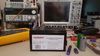
Typically removing the uncertainty in a DUT is only relevant when something goes wrong and you have to troubleshoot...the big 12v cell array is a very cost effective option for clean and predictable power....it's $100 vs a couple grand for a nice 30A linear tdk/lambda reference supply...the reference supplies still need to be characterized and nulled from the DUT. When dealing with vREF applied to a/d converters even running through multiple in line linear DC regulators won't solve a hard oscillation or other problem from a switching source...the linear Reg can smooth some noise but if the supply is oscillating sometimes the in line linear regulators won't have enough pre-bias to stabilize their junction and they can swing in junction resistance....thus can show up as a deviation down the line in the vREF driving the a/d
-
agreed....for end user application it's not relevant....for calibrations or analytics it is
-
Oh really? Can you elaborate on what sort of issues I might see? I just had a quick check on a few component sites and 12V 25+A linear supplies appear both to be rare, and horrendously expensive. So if it won't work out I'll just revert to using battery. But it'd be great to understand what might go wrong, so I can understand the risks and be on the look out for symptoms if I do go ahead. Thanks![/QUOTE] It depends on how good the isolation from AC is....again, the issue is the uncertainty induced from non-linear sources. From a pure research standpoint, we typically don't use switchers in development. We want to remove as much external influence as possible. Some "cheap" switchers can ring/oscillate at specific load levels (usually midpoint dead times). The best way around all of this is to fully decouple from AC and just use a good 12V battery. I personally like to use this....
-
I would recommend staying away from a switching supply, as it will not mimic the characteristics of a battery or linear supply....is the switcher has inadequate decoupling it will potentially oscillate and cause some issues.....there is simply not enough real estate on the dna200 board for enough capacitance on the input stage to smooth a "dirty/cheap" switching supply....traditionally when I do dev work on DC/DC systems, we try and stay away from any uncertainty in the current source....most switching supplies don't act as constant current devices, as a linear PSU or battery would....
-

What battery are you using/planning to use?
SSV replied to vaporlips's topic in Batteries and Charging
on such small aH capacity packs, I would highly recommend going to a LiFEpo4. With anything below 3000ish,maH you are going to be cycling VERY often. A traditional LiPo is not going to last very long, a LiFe is going to have MUCH greater cycle life, and it's energy density is still pretty good (120wH/kg). Also the benefits of safety, offered by lithium iron phosphate cells.....that will be my choice for research and development. Basically a 10aH "cased" cell array. You really want to have adequate current reserves for testing and calibrations..... -
I would love to have that command list as well....some automation would be very helpful in running PTC calibrations......is there a way to extract clock reference Via serial interface? This would be helpful when locking test gear (temp and resistance) + dna200 into matlab for time-correlated data-logging
-
I know it will save any wire manufacturer (with nothing to hide) a lot of time in customer service and training. Rather than try to explain to 99% of vapers how and why, just guide them to a profile. "Download it into your dna200 and here are optimum guidelines". This will solve a hell of a lot of un-necessary drama regarding "temp control issues" and blah blah blah....I know I am always happy to educate a user, but I can't reach everyone and I can only talk to them like an engineer. This has a lot of people avoiding the whole TC/TP concept, and for good reason. It seems overwhelming to them. I am sure everyone here can discuss the pros and cons of thermal mass and "speed", and RTD controller concepts, burden voltages etc....but when I start in with that on public forums, I am sure I lose 99% of the people who could have benefited from some form of temp protection/power throttling...
-
It's proprietary John.....I will PM, but I think the issue can be easily solved with some hysterisis in the range that the resistance "porpoises" I am going to demo the software/hardware as soon as it all lands and see if this non-linear behavior is a "problem"....our wire doesn't exhibit this until oxidation temps (900 deg C). However I can see some scenarios where there could be issues....being able to adjust that discreet range where one wire or another becomes non-linear, would be a HUGE benefit for my plans (possibly others). As my goal is to provide customers of our wires a "preset" for each unique product. A way to ensure that they can follow appropriate build guidelines with each of our wire products. For example we all know the massive discrepancy between YiHi chips and the dna40....in terms of accuracy. I am not so bothered that there is a temp offset, but more so bothered that the determination of sDEV between both devices is so wide. The dna40 is OBVIOUSLY more accurate, even with wires other than Ni200.....I would venture to say even more accurate than the evic VT in "Ti" mode (with titanium). The issue is not all titanium grades, or processing variations equal the same PTC. Obviously this goes for alloys of Titanium as well as diameter changes etc etc etc.... So being able to "correct" the baselines and scalars for each discreet property would be very beneficial to my intent. Thankfully we have the equipment to characterize these properties, but we still need a place to plug in the numbers....and account for some hysteresis....to combat non-linearities
-
Last winter, weren't there some people complaining that their DNA40s didn't work correctly if they were exposed to really low temperatures for a while? [/QUOTE] considering the metrology standard for calibrations is 27 deg C....I suppose they could have a valid problem....but they could always just breath really heavily onto their coils....might bring the resistance up enough to let the controller catch it (how awkward would the be.....)
-
on a slightly whimsical, side note.....is there provision for bottom of the range scalars of sub zero temperatures.....you know just in case someone wants to vape accurately in the frozen tundra ?
-
Alexander, have a look at the last post I made to you....I amended it with some more information on how we can solve these potential "issues".....this is a fairly common subject we encounter, when dealing with thermistors, thermo couples, and RTD controllers hysteresis is the name of the game =)
-
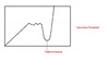
BAP, that's perfect....the exact info I was looking for.....the typical curve for our wire is represented in this "basic graph.....please excuse the crudity, it's for reference purposes only
-
Alexander, this is why I asked. You could track the tail (low side) of the sawtooth with a param for a "decrease" in resistance.....and implement a corrective lockout to NOT throttle power when that waveform is seen over X time. We do this quite often in other thermistors, when they reach saturation maximums and become non linear....I have a lot of experience with dc/dc controllers and we typically do this through hysteresis EDIT : here is a reasonably good article that might peak your interests https://sensorsandtransducers.wordpress.com/2012/02/07/thermistors/ because of the quantization of a 10 or 12 bit a/d the pure sine will be interpenetrated as a sawtooth.....in a 24 or 32 bit system we can get scalars that are more analogous to actual input waveforms, but I doubt it would be practical to implement a 24/32 bit a/d and associated vRef with any kind of stability in response....so we are stuck with interpolation errors, that look like a sawtooth thankfully most modern McU have a hysteresis object library, to correct for such "problems".....simply patching a hysteresis control algorithm into the DO loop can help "smooth" the curve
-
Our own wire products.....
-
John can you provide a datasheet or P/N for the thermistor used? i am curious about it's min/max thresholds....thanks in advance...
-
John so if I export thermocouple data, plus resistance data tend curves straight to .CSV (my equipment can lock to sample clock so the trends are time correlated) I can just bring that trend straight into eScribe? No hard scripting necessary? That would be very nice. Also can the software/firmware handle non linear points in the trend curve? Our wire has some unique properties at saturation.....it transitions from a linear PTC to a sawtooth when it hits temp saturation. So in essence I would like to have a calibrated scalar for each discreet wire product, that conforms to a reasonable degree of sDev accuracy across the coil surface. I am assuming this can easily be done with a traditional PTC scalar measurement method? Thanks, this is very good news indeed.
-
awesome....thank you....
-
I assumed this was the best place to ask, as other might want to know the same info....and a generalized response here will help evolv team save some time in answering the same dev questions over and over (via private replies)

